-
Tips for becoming a good boxer - November 6, 2020
-
7 expert tips for making your hens night a memorable one - November 6, 2020
-
5 reasons to host your Christmas party on a cruise boat - November 6, 2020
-
What to do when you’re charged with a crime - November 6, 2020
-
Should you get one or multiple dogs? Here’s all you need to know - November 3, 2020
-
A Guide: How to Build Your Very Own Magic Mirror - February 14, 2019
-
Our Top Inspirational Baseball Stars - November 24, 2018
-
Five Tech Tools That Will Help You Turn Your Blog into a Business - November 24, 2018
-
How to Indulge on Vacation without Expanding Your Waist - November 9, 2018
-
5 Strategies for Businesses to Appeal to Today’s Increasingly Mobile-Crazed Customers - November 9, 2018
Microsoft Finally Reveals HoloLens Processor Specifications
With Sony focusing so much on VR and is closing in on the release of PlayStation VR, many wonder why Microsoft never even bothered with VR. And according to the company, the future is Augmented Reality.
Advertisement
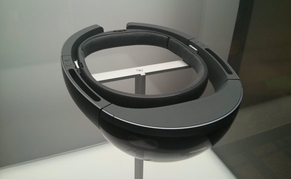
Windows 10 is expected to have a 3D desktop environment by 2017, so we might soon start to see Microsoft’s promise of enterprise-relevant HoloLens functionality beyond the endless promotional videos of architects and medics mucking around. The device is using awesome technology and power that transfers you to another dimension it seems.
During the annual Hot Chips conference in Cupertino, California, Microsoft pulled back the curtain on its secretive chip. It has two dozen Tensilica-brand digital signaling processing (DSP) cores with custom Tensilica Instruction Extension (TIE) instructions that allow new instructions to be added directly to the instruction set architecture (ISA). It also boasts 8MB of SRAM along with a layer of 1GB of low-power DDR3 RAM, all stuffed into a 12mm x 12mm BGA packages with a 0.4mm pitch.
Advertisement
The holographic processing unit is designed in such a way that it should be able to handle all the environment sensing and other input or output data necessary for proper functioning of HoloLens on its own. The HPU can perform roughly 1 trillion calculations per second, and the data it passes to the CPU requires little additional processing. Earlier in the year Microsoft published specs for the headset – it explained that the HoloLens was powered by the combination of a 14nm Intel Atom x86 Cherry Trail processor and a “Microsoft HPU”.


