-
Tips for becoming a good boxer - November 6, 2020
-
7 expert tips for making your hens night a memorable one - November 6, 2020
-
5 reasons to host your Christmas party on a cruise boat - November 6, 2020
-
What to do when you’re charged with a crime - November 6, 2020
-
Should you get one or multiple dogs? Here’s all you need to know - November 3, 2020
-
A Guide: How to Build Your Very Own Magic Mirror - February 14, 2019
-
Our Top Inspirational Baseball Stars - November 24, 2018
-
Five Tech Tools That Will Help You Turn Your Blog into a Business - November 24, 2018
-
How to Indulge on Vacation without Expanding Your Waist - November 9, 2018
-
5 Strategies for Businesses to Appeal to Today’s Increasingly Mobile-Crazed Customers - November 9, 2018
IBM thinks carbon nanotubes will defeat Moore’s law
IBM researcher Shu-Jen Han outlined the next challenges for carbon-nanotube transistors in a blog post.
Advertisement
After breaking through the 10-nanometer barrier, “IBM’s breakthrough in creating a new contact approach overcomes the other major hurdle in incorporating carbon nanotubes into semiconductor devices”, said IBM’s announcement on Thursday, October 1. The chips could be smaller and faster and significantly surpass what’s possible with today’s silicon semiconductors. IBM says making a transistor with a carbon-nanotube channel is relatively practical.
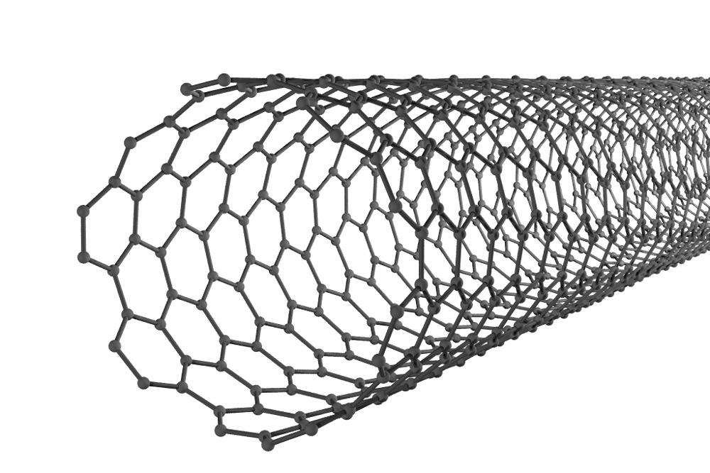
Earlier this year, an global consortium led by IBM disclosed development of a test chip with transistors as small as 7 nanometers – roughly 10,000 times thinner than a human hair. Graphene is a two-dimensional sheet of pure carbon (yes, one-atom-thick) that can conduct current well, but it does not have a bandgap, therefore, transistors made with graphene cannot be switched off. Carbon nanotubes are a rolled-up form of graphene, which are somewhat similar to Silicon since they both have band gap and can be used as the center piece of the transistor – the channel.
Electrons in carbon transistors can move more easily than in silicon-based devices, and the ultra-thin body of carbon nanotubes provide additional advantages at the atomic scale.
“You really don’t want the contact resistance to dominate in the device”, said Wilfried Haensch, an IBM research engineer. It’s now clear they can make the transistors as small as necessary, he says, and this is a big step toward the company’s goal of having carbon nanotube technology ready by 2020 (see “IBM: Commercial Nanotube Transistors Are Coming Soon”).
“We deposit them using a PVD [physical vapor deposition] process, then use high-temperature annealing-a metallurgical process akin to microscopic welding-to secure the channel contacts at each end”. The company sold off its last stake in silicon Power processor manufacturing to GlobalFoundries for $1.5 billion a year ago.
The contacts at the tips of a transistor control the flow of electrons off the device and into the channels of a CPU. This “end-bonded contact scheme” allows the contacts to be shrunk to below 10 nanometers without the performance of the carbon nanotube devices deteriorating.
“We’ve made great progress in purifying carbon, and we’re now within striking distance of the answers we need”, Gil said. A high-performance SWNT transistor was fabricated with a sub-10-nanometer contact length, showing a device resistance below 36 kilohms and on-current above 15 microampere per tube.
Above: A cross-section of a chip with IBM’s carbon nanotubes. They now sit between 11 and 14 nanometres, and anything closer to that would increase resistance to the point where the chip would start losing on performance.
Advertisement
Using this approach, the researchers in Yorktown Heights, N.Y., demonstrated the smallest contacts for carbon nanotubes at 9 nanometers, where the performance did not suffer despite the tiny dimensions. It involves bonding contacts made of molybdenum to the ends of the nanotube channel. And this year, Intel announced that the challenges and costs of bringing a new generation of technology to market had forced it to slow the torrid every-two-year pace it had been on for more than a decade.


